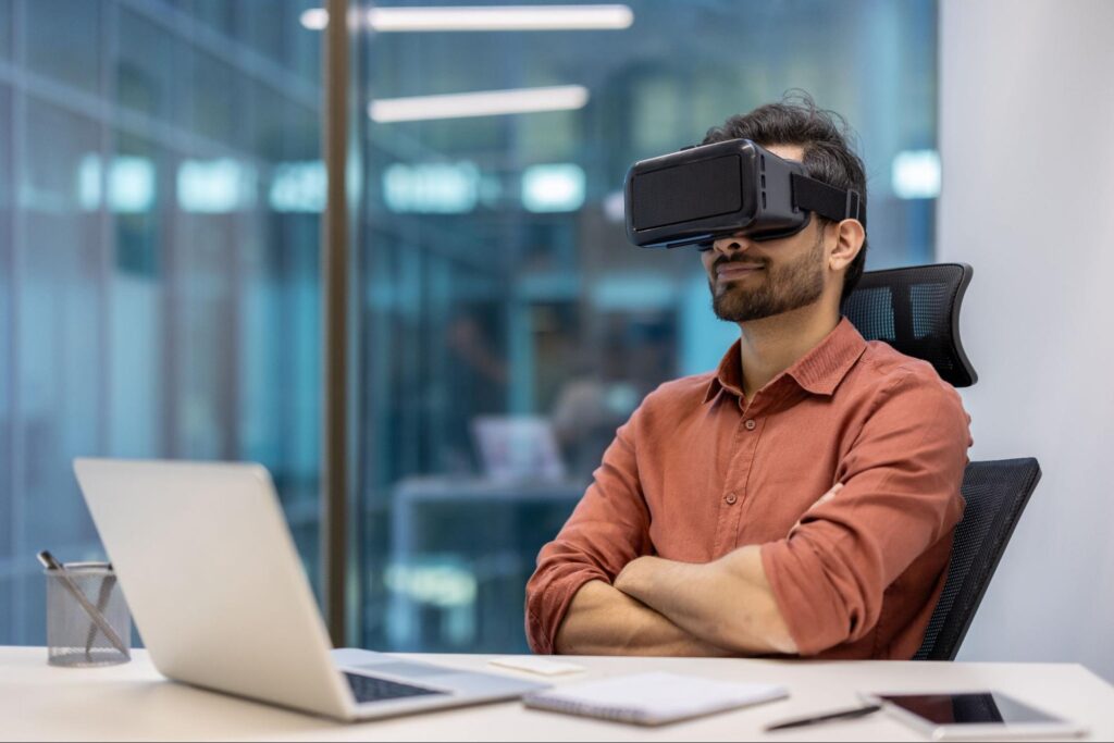
The U.S. semiconductor industry faces a looming shortfall of 60,000–100,000 skilled jobs by 2030, according to the NSF*. In response, virtual reality (VR) training and AI‑enabled simulations are emerging as key tools to spark interest, build skills, and deliver hands‑on experience, even for students without access to costly clean‑room labs.
But training alone isn’t enough. As students learn to assemble and test chip wafers, the real challenge begins: verifying internal assemblies, detecting hidden defects, and maintaining ultra‑tight tolerances. That’s where non‑destructive testing (NDT) and precision inspection tools become mission‑critical.
*Read more on the semiconductor’s industry shifts from the NSF here
How Virtual Training is Rewriting the Chip-Making Playbook
Programs supported by the NSF have used VR simulations to recreate actual chip‑fab clean‑rooms, enabling students to walk through manufacturing workflows step‑by‑step. These efforts are helping broaden the talent pipeline and give access to institutions that lack high‑end fabrication infrastructure.
Meanwhile, semiconductor manufacturers are facing a dual challenge: training talent and equipping that talent with tools that can perform at micron‑scale accuracy across inspection, test, and production operations.
Why Inspection & Imaging Tools Must Scale With Training
Virtual training builds awareness and foundational skills. But once technicians move into production or QA roles, they face hidden realities:
- Behind sensors, modules, and packaging are internal cavities, micro‑vias, bonding wires, and laminated stacks—many inaccessible without specialized imaging.
- Yield loss or failures often resolve back to “unseen” defects—voids in castings, delamination in stacks, corrosion under coatings, or micro‑cracks in assemblies.
- Traceability is essential: inspection systems must capture, export, and store images/videos tied to individual components and technicians.
In short: If training builds the workforce, then inspection tools empower that workforce to deliver quality at scale.
Inspection Best Practices for Semiconductor Environments
- Embed inspection early – Introduce borescope or NDT checks during training or prototyping so future operators recognize “what good looks like” from day one.
- Target hidden “failure zones” – Wiring harnesses, sensor modules, stacked packaging, and sealed assemblies all merit internal imaging rather than surface checks alone.
- Use high-resolution, exportable tools – Technicians need image clarity in tight spaces, plus documentation for audit trails.
Close the loop between training and metrics – Link inspection output with operator training records, yield data, and defect logs. - Keep tools portable and modular – Virtually trained technicians should be able to transition into real‑world fab floors or field operations with minimal ramp‑up.
How SPI Borescopes Supports Training‑To‑Inspection Workflows
At SPI Borescopes, we create inspection systems designed for high‑precision, tight‑space environments across aerospace, defense, industrial, and now manufacturing. Our tools offer:
- 4K imaging and ultra‑slim probes for seeing inside assemblies that technicians learn about in VR modules.
- Digital export and traceability so inspection data becomes part of the operator’s training record and quality dataset.
- Modular, field‑ready units that adapt easily from clean rooms to lab environments to production floors.
By integrating inspection technology into virtual training ecosystems, manufacturers can make training actionable and inspections measurable.
- Capture ultra-clear images inside tight cavities
- Operate under vibration, thermal cycling, and pressure changes
- Export inspection logs in flight-ready formats
- Support modular probe designs to reach complex geometries
When every inspection could be mission-critical, our tools help engineers see the unseen and trust the results when lives and billions of dollars are on the line.
TLDR:
The Outcome: A Stronger Workforce. Higher Quality. Lower Risk. Virtual training is essential for bridging the technician gap in semiconductor manufacturing. But for U.S. chip production to reach its full potential, inspection and imaging must keep pace. The future belongs to companies that not only train fast, but also verify deeply.
If you’re managing training programs, QA teams, or manufacturing readiness, now’s the time to ask:
- Are your trainees familiar with real‑world inspection tools?
- Do your inspection systems match the scale and complexity of modern assemblies?
- Is inspection data integrated with your training, quality, and production systems?
At SPI Borescopes, we help inspection engineers, training leads, and manufacturing teams bring clarity to the unseen. Want to see how our tools can integrate into your semiconductor process? Contact us today for more information, or request a free, hands-on demo.
Related Articles

A recent EASA survey found that aviation professionals are cautiously optimistic about AI in aviation safety, rating acceptance at 4.4 out of 7.

The FAA’s 2025 maintenance compliance updates introduce stricter documentation requirements, enhanced digital inspection tracking, and expanded training mandates for aerospace technicians.

In the aviation and aerospace industries, safety and reliability are paramount. Regular maintenance and rigorous quality assurance processes are critical to ensuring that aircraft operate efficiently and safely.